Junchuan Tang
Biography
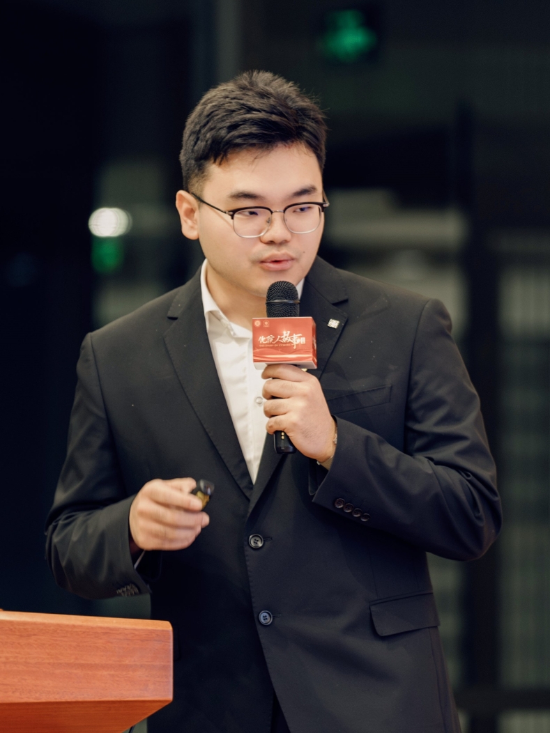
My name is Junchuan Tang, and I am currently a Ph.D. candidate in the College of Chemistry and Molecular Engineering (CCME) at Peking University. I began my undergraduate journey in the Chemistry program at Shandong University’s Taishan College and was fortunate to be recommended for admission to Peking University, where I am pursuing my doctoral studies under the supervision of Prof. Hailin Peng.
My research focuses on advanced transistor architectures based on two-dimensional semiconductors. I contributed to the development of the world's first epitaxial gate-dielectric integrated 2D FinFET and led the creation of the world’s first low-power 2D gate-all-around transistor. These works have been published at Nature, Nature Materials and Nature Review Electrical Engineering, and were recognized as part of the "Top 10 Scientific Advances in Semiconductors in China" and the "Top 10 Advances in Chip Science" in 2023.
I have been awarded the National Natural Science Foundation of China (NSFC) Youth Basic Research Program (for Ph.D. students) and have received numerous honors, including the National Scholarship, the Peking University President’s Scholarship, the Pioneer Scholarship, a nomination for Peking University’s Person of the Year Award, the Academic Innovation Award, and the “Star of Chemistry”.
Research experience
Throughout my research journey, I have encountered countless people and moments worth cherishing, but I owe particular gratitude to Dr. Congwei Tan (currently an Associate Research Fellow in the College of Chemistry). During my second year of doctoral studies, I had mastered most of the experimental techniques through persistent effort, but I still struggled to find a clear direction for my research. It was at this moment that Dr. Tan approached me. He admired my approach to problem-solving and invited me to collaborate on his project. At the time, he had made significant progress in the vertical growth of 2D fins but was facing challenges in constructing FinFETs. After reviewing his preliminary data, I made my decision in just five seconds: Let’s do it. We can make this work.
Once we set our goals, we broke the project down into manageable steps. For tasks requiring specific instruments, we sought access; for theoretical problems, we devoted ourselves to focused thinking; for repetitive experiments, we advanced in shifts. The semiconductor industry is rife with technological barriers, and China has long faced restrictions due to well-known reasons. However, while advanced lithography machines can be withheld, no one can stifle our unyielding creativity or the precision of the tweezers in our hands.
During the most intense months, Dr. Tan and I worked in relay: I would start at 10 a.m. and continue until 2 a.m., while he would pick up at 6 a.m. and work until 10 p.m. During overlapping hours, we collaborated on critical steps and discussed key issues. During our independent hours, we tackled the essential but repetitive tasks alone. Together, we overcame immense challenges and successfully developed the world’s first 2D FinFET for the 3nm technology node. This work was published in Nature and was recognized as one of the "Top 10 Scientific Advances in Semiconductors in China" and the "Top 10 Advances in Chip Science" in 2023.
However, the pace of semiconductor advancement is astonishing. Even during our submission period, more advanced “1nm” nodes were already being discussed in the International Roadmap for Semiconductors. This new node brought revolutionary changes in device architecture, leading to the emergence of the gate-all-around (GAA) structure. Industry leaders such as Samsung, Intel, and TSMC had already launched comprehensive efforts in this direction. Before I had the chance to celebrate our achievement, I was faced with an even greater challenge.

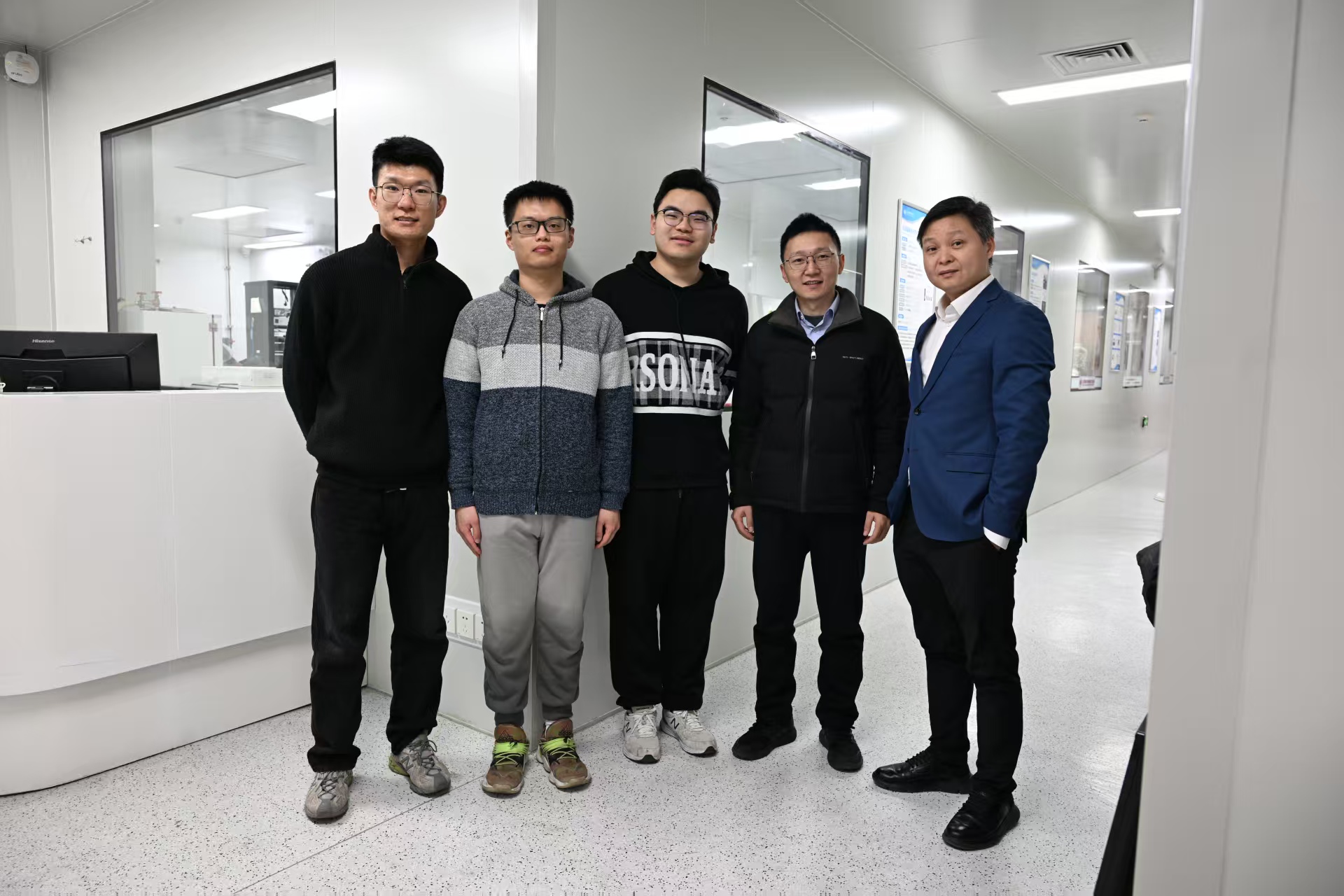
This time, Dr. Tan transitioned from being a close collaborator to a mentor who provided strategic guidance. The first third of the new project was conducted independently, and within six months, I had streamlined most of the fabrication processes. With the credibility of Peking University’s prestigious reputation, I was able to recruit collaborators with unique expertise.
Science has a way of attracting keen minds to new breakthroughs. Soon, the first collaborator joined with his expertise in electron microscopy. The second, Jianfeng Jiang (currently a postdoctoral researcher at MIT), joined in October of last year. The final collaborator, Gao Xin (now a Boya Postdoctoral Fellow at Peking University), came aboard this March. At the start of this year, we successfully pioneered the world’s first low-power integrated 2D GAA transistor, filling a critical gap in the field. This cutting-edge transistor, independently developed by Peking University, broke through international technological barriers. Its performance and energy efficiency surpassed those of leading companies like Intel, TSMC, and IMEC, earning accolades from both industry authorities and competitors, which published and highlighted by Nature Materials. Our work was reported on the front page of Guangming Daily, and reprinted by People's Daily, Guangming Net, Sohu.com, Peking University official, Peking University News network, etc. This work also helped me secure funding from the inaugural National Natural Science Foundation’s doctoral program.
After achieving a breakthrough with the prototype device, I am now leading a team of newcomers to seize this momentum and conduct further research aimed at advanced integrated circuits.


