Scaling down the size of field-effect transistors (FETs) in integrated circuits leads to higher switching frequency and integration density, but also results in degraded switch-off behavior due to the short-channel effects. To mitigate these effects, transistors made of high-mobility two-dimensional (2D) semiconductor channels and ultrathin dielectrics with sub-0.5-nm-EOT (equivalent oxide thickness), are required by the International Roadmap for Devices and Systems (IRDS). However, the integration of both is still challenging. Recently, Hailin Peng group reported the synthesis of a single-crystalline native oxide dielectric, β-Bi2SeO5, via an ultraviolet-assisted intercalative oxidation of high-mobility 2D semiconductor Bi2O2Se. Single-crystalline β-Bi2SeO5 has excellent insulativity and high dielectric constant of around 22, and can be scaled down to an EOT of 0.41 nm in 2D FETs, with leakage current below the low-power limit, meeting the requirements of IRDS. This research entitled “A single-crystalline native dielectric for two-dimensional semiconductors with an equivalent oxide thickness below 0.5 nm” has been published by Nature Electronics on Sept. 15th, 2022.
Scaling down the size of field-effect transistors (FETs) in integrated circuits leads to higher switching frequency and more devices integrated on a single chip. However, when the length of the semiconductor channel is less than 6 times the characteristic length, the switch-off behaviour is degraded due to the short-channel effect, leading to a reduced frequency and higher power consumption. The characteristic length is defined as: = ![]() , where n is the effective gate number, and tb (εb) and tox (εox) are the thicknesses (dielectric constants) of the semiconductor body and oxide dielectric, respectively. Thus, using transistors made of two-dimensional (2D) semiconductor channels and ultrathin dielectrics with high dielectric constant can minimize and mitigate the short-channel effects.
, where n is the effective gate number, and tb (εb) and tox (εox) are the thicknesses (dielectric constants) of the semiconductor body and oxide dielectric, respectively. Thus, using transistors made of two-dimensional (2D) semiconductor channels and ultrathin dielectrics with high dielectric constant can minimize and mitigate the short-channel effects.
However, it remains a challenge to integrate 2D semiconductors with dielectrics that have sub-0.5-nm EOT (equivalent oxide thickness) and low leakage current, as required by IRDS. Dielectrics on 2D semiconductors, including HfO2, hBN and CaF2, cannot be scaled down to an EOT of less than 0.9 nm, owing to issues such as poor insulativity or low dielectric constant. Thus, a new ultrathin dielectric with high dielectric constant and excellent insulativity is urgently required for 2D electronics.
Prof. Hailin Peng group developed a high-mobility 2D semiconductor Bi2O2Se (Nature Nanotechnology 2017, 12, 530), and have been working on the oxidation of Bi2O2Se. Bi2O2Se has been transformed into polycrystalline or amorphous native oxide dielectric Bi2SeO5 via thermal oxidation (Nature Electronics 2020, 3, 473) or oxygen plasma treatment (Nano Letters 2020, 20, 7469). High-performance 2D Bi2O2Se FETs and inverter circuits were fabricated (Acc. Mater. Res. 2021, 2, 842-853), in which the native oxide dielectrics can be scaled down to an EOT of 0.9 nm.
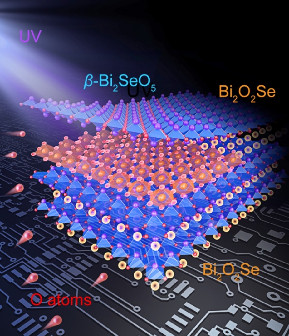
Fig. 1 Diagram of the UV-assisted intercalative oxidation of 2D Bi2O2Se for single-crystalline native oxide dielectric β-Bi2SeO5.
Recently, inspired by the zipper-like layered structure of 2D Bi2O2Se and the intercalation of 2D materials, Peng’s group developed an UV-assisted intercalative oxidation process of 2D Bi2O2Se (Fig. 1). The Bi-O framework of the precursor remains intact throughout the process (Fig. 2a), and thus the native oxide dielectric, a new phase of Bi2SeO5 (named β-Bi2SeO5), inherits the single-crystalline characteristic of the Bi2O2Se precursor. The UV-assisted intercalative oxidation is compatible with UV lithography, and with a special lithography mask, wafer-scale area-selective oxidation can be achieved (Fig. 2b). 2D Bi2O2Se can also be oxidized layer-by-layer, and an atomically-flat lattice-matched interface can be obtained.
The single-crystalline β-Bi2SeO5 can serve as a high-performance dielectric in Bi2O2Se-based 2D FETs, owing to the atomically-flat lattice-matched interface, thickness-independent high dielectric constant of around 22, and excellent insulativity. 2D transistors fabricated with β-Bi2SeO5/Bi2O2Se heterostructure show high electrical performance, including a mobility of 427 cm2·V–1·s–1, hysteresis as low as 20–60 mV, and subthreshold swing (SS) below 65 mV·dec–1. In addition, even the thinnest β-Bi